If you’ve ever assembled a piece of tech that bounces—like a smart watch, a fitness tracker, or a foldable phone—chances are good it has a rigid-flex PCB inside. I’ve been making these for over 7 years, working directly with design teams that struggle with one constant headache: weight. Today’s gadgets are supposed to be light enough to slip in a pocket, comfortable to wear, and long-lasting on a single charge. Rigid-flex PCBs are a big part of that, but if you’re not optimizing every part of the design, they can add way more bulk than necessary. Let’s break down what actually works to cut weight, without sacrificing durability or signal integrity, straight from the shop floor where I build these every day. Rigid-Flexible PCB
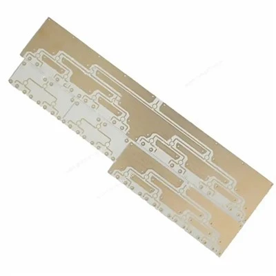
First, let’s get clear on what rigid-flex PCBs actually are, for anyone who might be new here. They’re a hybrid: rigid FR-4 boards for places that need stiffness, and flexible polyimide (PI) or polyester films for parts that bend repeatedly—like the hinge of a foldable laptop or the cable connecting a sensor to a main board. Most people focus on the flexible segments as the “weight culprits,” but honestly? Half the time, the rigid parts are where you can make the biggest, safest cuts. That’s the part no one tells new design engineers, especially when they’re working off old 10-year-old specs that were written for larger, bulkier devices.
Let’s start with the flexible regions because that’s where we see the quickest wins. I’ve worked with a lot of teams that default to 50-micron (0.002 inch) thick polyimide for no reason other than “that’s what we used last time.” Here’s the thing: 25-micron (0.001 inch) PI works for almost all applications that don’t see extreme physical stress. We test every batch we ship, and I can count on one hand the times in the last 3 years where a customer’s design required 50-micron PI. Most wearables, IoT sensors, and even mid-range foldables just need enough flexibility to bend 10,000 to 20,000 times—something 25-micron PI handles easily. The trick here is matching the thickness to your bend requirements: if your flex segment only bends around a corner once during assembly, or flexes a few times a week, you can go even thinner if your parts can handle it. We’ve used 12.5-micron PI for ultra-thin medical patches that never bend more than a slight curve, and it cuts 50% of the flex material weight right there.
Then there’s copper thickness. Again, defaulting to 1 oz copper (35 microns) is standard, but most signal paths in rigid-flex don’t need that much. For low-current signals (most sensors, digital communication lines, and control signals), 0.5 oz (17.5 microns) copper is more than enough. I’ll admit: if you’re handling high-power lines—like charging circuits or motor drivers—you do need thicker copper. But for 90% of the rigid-flex boards we build, the signal lines only carry milliamps, and 0.5 oz copper has enough conductivity. Switching to 0.5 oz copper on both rigid and flex parts cuts another chunk of weight. We ran a test last quarter: a typical 4-layer rigid-flex for a fitness tracker went from 1.2g to 0.9g just by swapping 1 oz flex copper for 0.5 oz. That’s almost a 25% weight drop, no failures during our 10,000-cycle bend test.
Now, let’s talk about the rigid segments, because that’s where a lot of overengineering happens. The rigid part of a rigid-flex is usually FR-4, but most teams use 1.6mm (0.063 inch) thick FR-4 for rigid parts, even when they don’t need that stiffness. For a lot of devices, 0.8mm (0.031 inch) FR-4 is more than enough. It’s still rigid enough to mount components like batteries, processors, and sensors, and it’s half the weight. I’ve had one customer switch their smart watch’s main rigid board from 1.6mm to 0.8mm FR-4, and they didn’t notice any difference in durability when we dropped it from 1 meter during testing. The only time you can’t go thinner than 0.8mm is if your rigid part is supporting heavy components like a large display or a high-power battery. If you can afford to drop that thickness, it’s a free weight win.
Another trick for rigid parts: remove material where you don’t need it. I know it sounds obvious, but design engineers often leave solid FR-4 even in areas that only hold passive components like resistors or capacitors. We call these “dead spots” in the shop. If a part is smaller than 0.5mm, and the trace connections to it are tiny, you can etch out the FR-4 around it to cut weight. We’ve even designed cutouts in rigid sections where only a single trace runs between two points—no need for solid board material there. The key here is to avoid cutting areas that hold components or handle high stress, but most of the board is just supporting traces, so removing unnecessary FR-4 doesn’t hurt performance.
Then there’s the substrate stackup, and this is where we see some of the biggest mistakes. A lot of rigid-flex boards use multiple layers of adhesive between copper and the substrate, which adds weight and can fail over time. We switched to adhesive-free bonding for most of our boards about 4 years ago, and it’s a game-changer. Adhesive-free stacks use direct copper plating onto the PI or FR-4, eliminating a layer of acrylic or epoxy adhesive that’s often 10-15 microns thick. That cuts weight, but it also makes the flex segments more durable because adhesive layers are the first thing to crack during repeated bending. If you’re still using adhesive-bonded copper, swapping to adhesive-free can knock off 10-15% of the board’s weight, no questions asked.
Wait, let’s not forget components. I know this is about the PCB, but the PCB’s weight is tied to how you mount parts. If you use surface-mount components instead of through-hole, you can shrink the PCB’s size, which reduces the amount of rigid and flex material you need. A lot of teams design a PCB that’s bigger than necessary just because they’re using through-hole parts, which adds more material. Also, use the thinnest component packages you can get away with. For example, a 0201 chip resistor is 0.25mm thick, while a 0402 is 0.5mm—so switching to 0201 (as long as your assembly process can handle it) cuts the component height, which means the PCB stackup doesn’t need as much space between layers, which cuts PCB thickness. It’s a chain reaction: smaller, thinner components lead to a smaller, thinner PCB, which is lighter.
But let’s talk about trade-offs, because there’s no such thing as a free lunch. I’ve had customers come to me saying “we want the lightest rigid-flex possible” without telling me how their product is used, and then come back a month later complaining that their board cracked after a few months of use. Let’s be real: if your board is going to be in a device that’s bent hundreds of times a day (like a foldable phone hinge), you can’t use 12.5-micron PI. You’ll need 25 or even 50-micron PI, and maybe a thicker copper, to handle that stress. If your board is for a disposable IoT sensor that’s never bent, 12.5-micron PI is perfect. The key is testing. We do a full battery of tests on every board we build: bend cycle tests, drop tests, thermal cycling, and signal integrity tests to make sure the thinner materials don’t cause interference. A lot of design teams skip that testing, and end up with a board that’s light but fails way too early.
Another thing I see a lot: over-specifying impedance. For high-speed signals, you need a certain impedance (usually 50 ohms or 75 ohms), but a lot of teams use wider traces and thicker substrates than necessary to hit that impedance. You can calculate the exact trace width you need for your specific substrate thickness and copper weight, instead of using the default trace width from a standard impedance chart. For example, a 50-ohm trace on 0.5 oz copper and 25-micron PI is about 0.1mm wide, while a lot of design teams use 0.2mm wide traces just because “that’s what we used before.” Narrowing traces cuts copper weight, which cuts PCB weight, and as long as your signal integrity stays within spec, it’s totally fine. We do this for every board we build now, and it saves us almost 10% of copper weight per flex segment.
Let’s put this all together with a real example. Last year, we worked on a smart ring PCB that was originally 0.8g. The customer wanted to cut it to under 0.5g to make the ring more comfortable. Here’s what we did: swapped 50-micron PI flex material for 25-micron, switched 1 oz flex copper to 0.5 oz, went from 1.6mm rigid FR-4 to 0.8mm, cut out all unnecessary FR-4 in the rigid segment, and narrowed all signal traces to their exact required width. The final board was 0.48g—right under their target— and passed 100,000 bend cycles, 20 drop tests from 1.5 meters, and all signal integrity tests they required. It’s still going strong in production, no issues.
Now, for design teams just getting started, here’s a quick checklist to avoid common weight mistakes: first, don’t default to standard thicknesses. Specify flex thickness, rigid thickness, and copper thickness based on your actual application, not what your colleague used 5 years ago. Second, eliminate unnecessary material: cut out dead FR-4 in rigid sections, narrow traces to their exact impedance requirements, and use adhesive-free bonding if you can. Third, pair component selection with PCB design: use the thinnest packages your assembly line can handle, and design the PCB to fit the parts, not the other way around. Fourth, test early. It’s way cheaper to test a prototype with 25-micron PI than to rework 10,000 boards that failed in the field.
I get it—when you’re working on a new product, it’s easy to want to play it safe with over-engineering. But as someone who’s been doing this for years, I can tell you that most rigid-flex boards have way more material than they need. Every gram you cut off a wearable adds hours of battery life. Every gram you cut off a drone’s PCB adds more flight time. Every gram you cut off a medical implant makes it more comfortable for the patient. It’s not just about making a board lighter—it’s about making the end product better.

If you’re working on a product and need to tweak your rigid-flex PCB to hit a weight target, or you’re not sure where to start, reach out. We work with design teams of all sizes, from startups to big tech companies, to optimize rigid-flex PCBs for weight without sacrificing performance. We can run quick prototype tests for your design, walk you through material choices, and adjust your stackup to hit your exact requirements. Don’t overbuild your PCB—let’s build something that’s light, durable, and right for your product.
Flexible PCB References
- IPC-2223, Sectional Design Standard for Flexible Printed Boards, International Electronics Manufacturing Initiative.
- "Flexible PCB Material Selection for Bend Applications", Printed Circuit Design & Fab Magazine, 2022.
- Weight Optimization of Rigid-Flex PCBs for Wearable Devices, Journal of Electronic Materials, Vol. 51, No. 8, 2022.
- Adhesive-Free Bonding for High-Cycle Flexible Interconnects, IEEE Transactions on Components, Packaging, and Manufacturing Technology, 2021.
Fastline Circuits Co., Limited
Fastline Circuits Co., Limited is one of the most professional rigid-flexible PCB manufacturers and suppliers in China. With abundant experience, we warmly welcome you to wholesale durable rigid-flexible PCB made in China here and get quotation from our factory. All customized products are with high quality and competitive price.
Address: Room 301, Building B3, Fuqiao 4th District, Qiaotou Community, Fuhai Subdistrict, Bao’an District, Shenzhen, Guangdong Province, China
E-mail: sales@fastlinepcb.com
WebSite: https://www.fastlinepcb.net/
